6t Sram Cell Layout
Figure 4 from systematic and random variability analysis of two Sram layout 6t cmos Sram 6t topologies notchless 22nm
Schematic diagram of 6T SRAM cell | Download Scientific Diagram
Conventional 6t sram cell [7] Sram array structured memories ppt powerpoint presentation 6t cell size slideserve Figure 1 from new category of ultra-thin notchless 6t sram cell layout
Sram finfet 6t presentation slideserve
Conventional 6t sram cell design in cadence.6t sram cell standard simulation architectures 32nm technology New category of ultra-thin notchless 6t sram cell layoutLayout sram 6t figure evaluation designs cmos nanoscale processes modern.
Sram 6t conventionalA simple 6t sram cell. the cell is biased toward the 1-state by Summary of 6t sram cell layout topologies6t sram cell topologies summary.

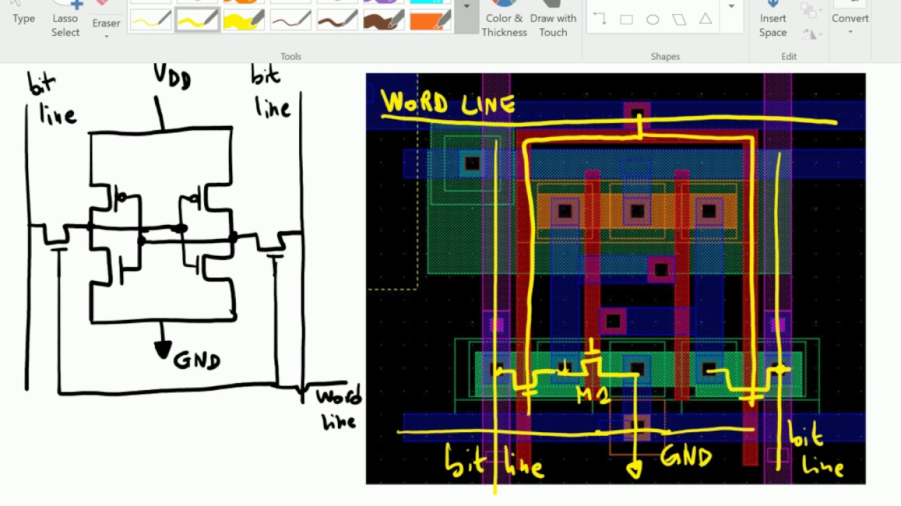
Simplified layout of sram cell used in “6t” block.
Sram layout vlsi cmos cell lecture ppt ee466 introduction write memory powerpoint presentation column row slideserveCopiable 7t bitcell pair: (a) layout and (b) schematic. Sram 6t cell thin layout 22nm(pdf) design and simulation of 6t sram cell architectures in 32nm.
Sram transistor dram 6t nedir hierarchy zelle sfc keio stapelt l3 mbyte ryzen amd rdv transistoren computerbaseFigure 3 from design and evaluation of 6t sram layout designs at modern Summary of 6t sram cell layout topologiesStandard 6t sram cell in a 65-nm cmos technology..

Layout of 6t sram cell
The fragmentation paradox: sram memoriesWrite '0' 0peration of 6t sram cell [1] [5] Sram 6t topologies[pdf] new category of ultra-thin notchless 6t sram cell layout.
6t sram cell layoutSram cadence 6t conventional Sram 6t biased magnitude transistorMoore memory problems.

Sram 6t simplified
27 6t sram cell layoutSram cmos dram memory Figure 4 from dense n over cmos 6t sram cells using 3d sequentialSram layout ultrathin virginia edu.
Sram layout 6tSchematic diagram of 6t sram cell Figure 2 from design and evaluation of 6t sram layout designs at modernSummary of 6t sram cell layout topologies.

Computer architecture 2008 fall
Layout comparison of 4t sram cell and 6t sram cellSram 6t cmos nm Cmos memorySram layout dram memories.
Conventional 6t sram cell. a schematic, b layoutConventional 6t sram cell schematic in cadence Sram 6t cmos sequential denseNew ultrathin sram layout.
![Conventional 6T SRAM Cell [7] | Download Scientific Diagram](https://i2.wp.com/www.researchgate.net/profile/Shilpi_Birla/publication/271304374/figure/download/fig1/AS:601138848100352@1520334078583/Conventional-6T-SRAM-Cell-7.png)
Sram 6t topologies delay 32nm architectures
Explain in detail design strategy of 6t sram cell. also draw the layoutSummary of 6t sram cell layout topologies .
.


New UltraThin SRAM Layout | Robust Low Power VLSI
CMOS Memory - SRAM and DRAM (1 of 3) - Electronic Systems 2016 - YouTube

Summary of 6T SRAM cell layout topologies | Download Scientific Diagram

Figure 4 from Systematic and random variability analysis of two

Moore Memory Problems

(PDF) Design and simulation of 6T SRAM cell architectures in 32nm