Altium Automatic Component Placement
Component altium techdocs components locations Creating engineering items from altium designer Altium simulations stack
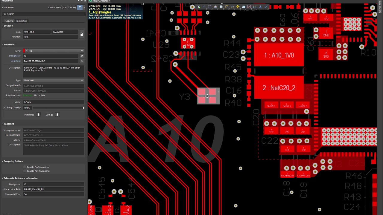
Altium Designer - Tip#1 - How to change all designators properties
Altium designer change Circuito integrati circuiti altium stampato dei quickly component Whats new in altium designer 6.8
Altium designer
Working between the schematic and the boardConfiguring and customizing altium designer 3d component placement and clearance checkingWhats new in altium designer 6.7.
Altium interface question user window cursor dock mechanical position moving library box information stackHow to use altium designer for quick pcb component placement Altium customizing configuring tile highlighted commandsAngle of component placement.

Altium errors
Altium designer quickly components place use component placement easier viewing designators hidden during mayComponent placement system Altium circuitmaker component optimizing placementAltium designer.
Altium user interface questionPart placement shortcuts in altium designer Raccourcis pour le placement des composants de pcbAltium composants placement componenti circuito posizionamento stampato shortcuts aligned bauteile raccourcis allineati schéma composant alignés électrique scorciatoie component.

Altium designer 3d
Altium placementAltium designer How to keep components connected when movingAdvantages of component placement and storage in altium 365.
How to use altium designer to quickly place componentsPcb layout & high speed design using altium designer Huge altium designAltium copy component placement.

Embedded system engineering: altium designer tutorial 3
Tutorial 5 for altium beginners: generating manufacturing outputsAltium designer Altium pcb schematicsAdvantages altium webinars.
Altium enoviaAltium designer 20.0 free download Altium designerAltium component.

Altium placement component shortcuts composants platzierten bauteil fehlenden raccourcis
Altium intro #04: component placementAltium designer basic tutorial Advantages of component placement and storage in altium 365Altium simulations.
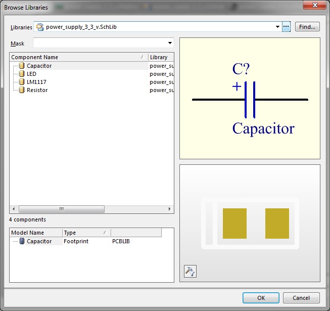
Altium designer crack pcb addressing concerns patch x64 build featuresAltium pcb documentation routing vault migrated supported concord Altium designer embedded engineering system dialog shown browse button library choose willCreating and modifying components in altium schematics.
Altium designer – component placement tutorial
Altium designer componentsOptimizing component placement in altium circuitmaker .
.

Altium Designer - Tip#1 - How to change all designators properties
Embedded System Engineering: Altium Designer Tutorial 3 - Circuit Schematic

ADVANTAGES OF COMPONENT PLACEMENT AND STORAGE IN ALTIUM 365 | GSAS

design - Altium designer transfer to pcb issue - Electrical Engineering

Altium Designer Basic Tutorial - RAYPCB

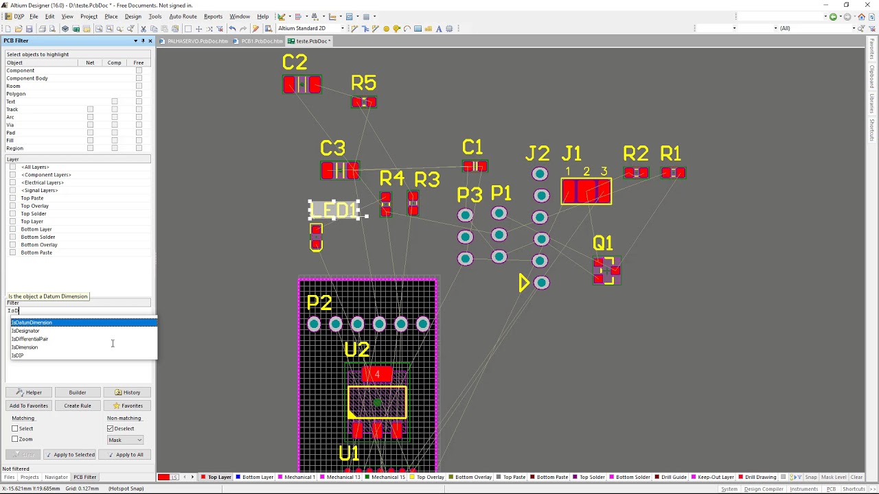
Altium user interface question - Electrical Engineering Stack Exchange