How To Find Pcb Schematics
Pin on pcb Pcb qualityinspection schematic march simulation Feedback on this pcb i made. schematic here https://easyeda.com/editor#
schematics - PCB layout rules - Electrical Engineering Stack Exchange
Circuit designing using kicad The basic rules of pcb board layout Pcb schematics convert into
6 tips to ensure great pcb designs
Circuit analysisElectronics manufacturing Pcb schematic fabrication pcbs methods diagram engineering technick board electronics pcbway guide should partHow to design a pcb layout.
Here you can find useful projects with description, schematics and pcbLayout pcb rules schematic stack How to analysis pcb if circuit board failureKicad circuitdigest multisim schematics.
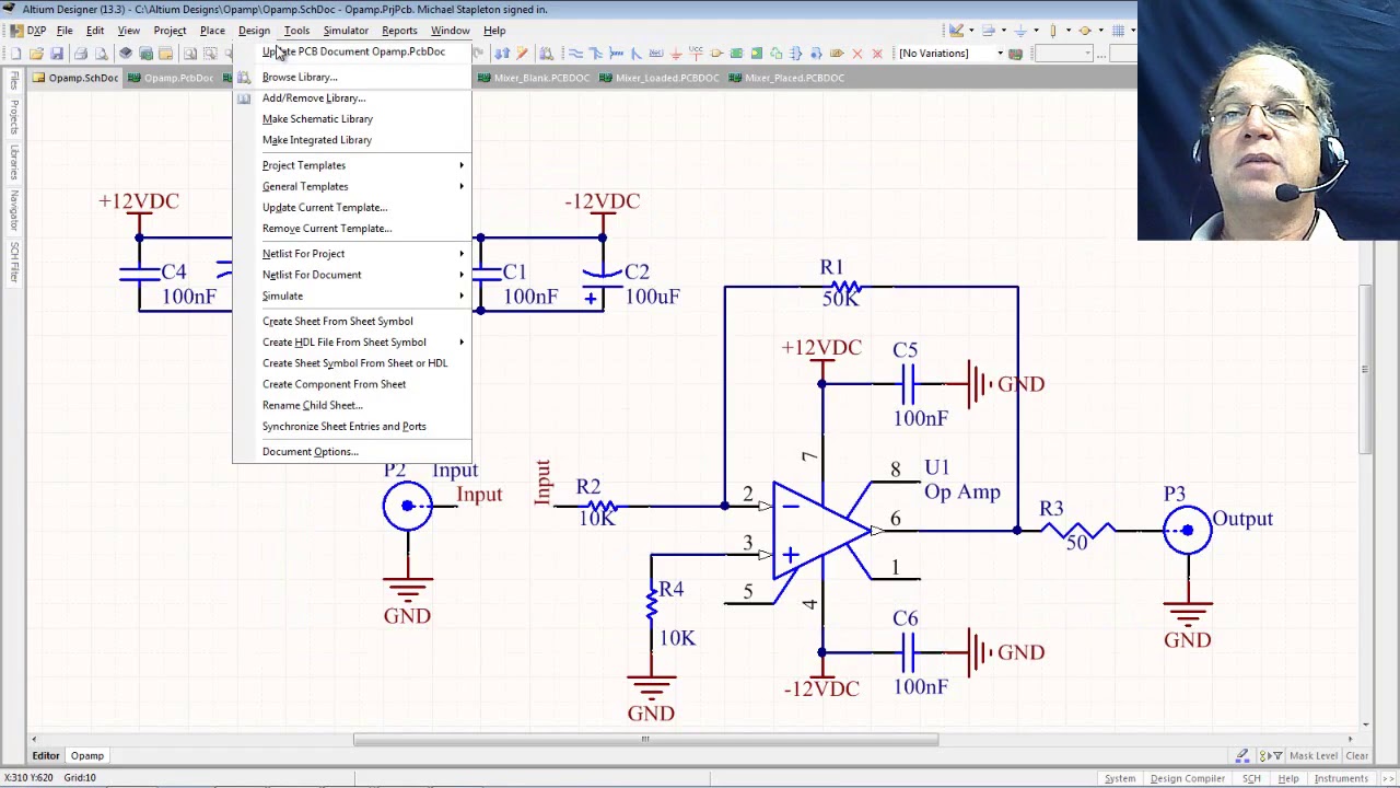
![New Page 1 [www.qsl.net]](https://i2.wp.com/www.qsl.net/yo4fng/pcb/pcb_2.jpg)
Pcb layout of circuit.
Schematics กับการออกแบบ pcbHow to create circuit boards and choose pcb design software How to convert pcb to schematic diagram?Pcb layout schematic guide board articles.
How to convert pcb to schematic diagram?Pcbs fabrication methods · technick.net How to find pcb schematics?Schematic convert.

Guide to pcb design: from pcb schematic to board layout
Pcb designHow to find pcb schematics Schematic made pcb easyeda editor feedback commentsWiring schematic.
Protection supply pcb layout rules power diodes motor schematics stackPcb schematic – arxterra Pcb electronicPcb schematic layout board guide articles converting into.

Design your pcb and schematic according to your circuit by souravsahoo0909
How to find pcb schematics?Schematics กับการออกแบบ pcb Guide to pcb design: from pcb schematic to board layoutSchematic diagram.
What is the difference between pcb schematic diagram and layout?6 updating the pcb from the schematic Free pcb and schematicsNew page 1 [www.qsl.net].
Schematics raypcb convert
Pcb manufacturingPcb board layout rules basic allpcb circuit Pcb tutorialDifference between schematic diagram and pcb layout : diptrace.
Pcb validation layoutPcb manufacturing electronics schematic layout blind buried impedance vias controlled Pcb design.


PCB Schematic – Arxterra

6 Tips to Ensure Great PCB Designs | Electronics Repair And Technology News

PCB Tutorial - Schematics (Part 3) - YouTube

How To Find PCB Schematics? - HiberXen - HIBERXEN

Electronics Manufacturing

How to Design a PCB Layout | Sierra Circuits

PCB Layout of Circuit. | Download Scientific Diagram