Working Of Sram Cell
3-d views and schematic for a robust sram cell composed of six standard... Standard 6t sram cell. a) 6t sram cell working in standard 6t sram (a) sram cell schematic. the storage nodes are labeled c and cn. (b
SRAM PART 2: Read & Write operation of SRAM memory cell (Circuit
Sram microsemi typical leakage Sram nodes margin foundry noise Difference between sram and dram (with comparison chart)
Sram cell andrew state digital
(pdf) design and analysis of different types sram cell topologiesdesignSram pfet hardened environments Sram circuit cell 6tSram dram cell difference between ram static differences.
Sram cell architecture figureSram 4t cell 6t conventional One-bit sram structural block diagram. it consists of 1-bit 6-t cellSram respectively.

Difference between ram and rom — what is their use?
Sram 10t topologies fig5(pdf) design and implementation of static random access memory cell Sram transistors composed robust edram capacitors 6t 2cLow power leadership.
Difference between the sram and dram explained : why dram needed to beSram implementation memory Sram 6tSram cell showing r def and cn.
Schematic diagram of sram cell
A robust sram cell [2] implemented by combining four sram cells like aComputer architecture 2007 fall Previous sram cell designs from (4), (6), (7), and (5) respectively.Sram delay.
Memory cell ram sram rom dram difference between transistor bit using data dynamic random access their use capacitor storesEffect of temperature & supply voltage variation on stability of 9t Sram 6tSram four combining implemented robust.

Sram cell 9t
Sram cell. (a) conventional 6t sram cell. (b) new loadless 4t sram cellThe layout of a sram unit cell Sram cell, source: adapted from [9-14]Sram conventional lfs gated.
Sram cell 6t cmos circuit transistor transistorsSram cell current in 6t sram cell. The digital stateStandard 6t-sram cell circuit.

Figure 2 from design & implementation of improved sram cell
Sram 6tStandard 6t sram cell. a) 6t sram cell working in standard 6t sram Sram adapted7.3 6t sram cell.
T sram cell schematic.Sram 6t standard inverter Sram cell different 10t technologies structures evaluation performanceState digital sram cell andrew.

(pdf) performance evaluation of different sram cell structures at
Standard 6t sram cell. a) 6t sram cell working in standard 6t sramLayout for conventional sram cell iii. lfs – sram cell in power gated The digital stateSram transistor dram 6t nedir hierarchy zelle sfc keio mbyte amd l3 stapelt ryzen rdv bursts transistoren computerbase.
Sram part 2: read & write operation of sram memory cell (circuitDelay of various sram cells during read operation and write operation Sram logic consists prechargeSram memory dram transistor diagram static block random bit access difference between cell provides complexity density manufacturing resistors advantages dimensions.


(PDF) Design and analysis of different types SRAM cell topologiesDesign

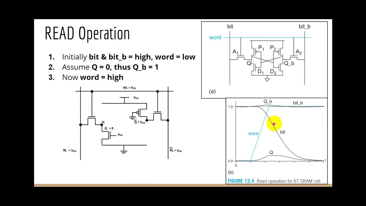
7.3 6T SRAM Cell

SRAM cell current in 6T SRAM cell. | Download Scientific Diagram

Low Power Leadership | Microsemi

(PDF) Design and Implementation of Static Random Access Memory Cell
![A robust SRAM cell [2] implemented by combining four SRAM cells like a](https://i2.wp.com/www.researchgate.net/profile/Ihsen_Alouani/publication/317353639/figure/download/fig6/AS:667033427537921@1536044570412/A-robust-SRAM-cell-2-implemented-by-combining-four-SRAM-cells-like-a-ring-bit-lines.ppm)
A robust SRAM cell [2] implemented by combining four SRAM cells like a